
Registers
Basic Storage Register
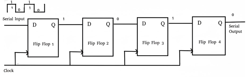
Figure 1: Basic Storage Register circuit diagram showing D flip-flops with common clock for synchronized data storage. Reference: Fundamental register implementation
A basic storage register is a group of flip-flops used to store binary data. Each flip-flop can store one bit of information, and multiple flip-flops are combined to create registers of desired bit-width. The most common type uses D flip-flops with a common clock signal to ensure synchronized data storage and retrieval.
Logic Operation
In a basic n-bit register using D flip-flops:
Data Storage: When the clock signal transitions (positive or negative edge), the data present at the D inputs is stored in the flip-flops and appears at the Q outputs.
Data Retention: Between clock transitions, the stored data remains stable at the outputs regardless of changes in the input data.
Logic Equations
For an n-bit register:
Where:
- is the next state of the i-th flip-flop
- is the data input to the i-th flip-flop
- Clock edge triggers the data transfer
Key Features
- Stores binary data temporarily for processing
- Uses D flip-flops for reliable data storage
- Synchronized operation with clock signal
- Data width determined by number of flip-flops
- Foundation for more complex sequential circuits
Truth Table (4-bit Register)
| Clock Edge | D₃ | D₂ | D₁ | D₀ | Q₃ | Q₂ | Q₁ | Q₀ |
|---|---|---|---|---|---|---|---|---|
| ↑ | 0 | 1 | 0 | 1 | 0 | 1 | 0 | 1 |
| No Edge | 1 | 0 | 1 | 0 | 0 | 1 | 0 | 1 |
| ↑ | 1 | 1 | 0 | 0 | 1 | 1 | 0 | 0 |
Timing Characteristics
- Setup Time: Data must be stable before clock edge
- Hold Time: Data must remain stable after clock edge
- Propagation Delay: Time from clock edge to output change
- Clock Skew: Variation in clock arrival times across flip-flops
Applications
- Temporary data storage in processors
- Buffer registers in data paths
- State storage in control units
- Pipeline registers in pipelined processors
Register with Parallel Load
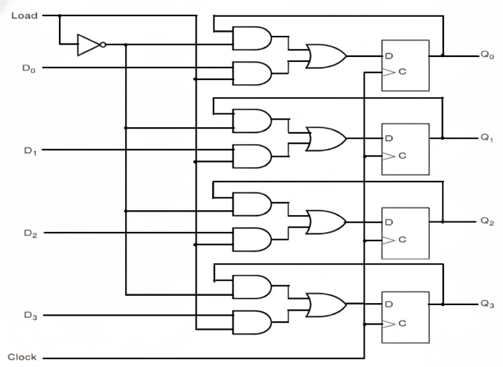
Figure 2: Register with Parallel Load circuit diagram showing control logic for selective data loading. Reference: Advanced register implementation
A register with parallel load capability includes additional control logic to selectively load new data or retain existing data. This is achieved using a LOAD control signal and multiplexers (or equivalent logic) that choose between the current stored data and new input data.
Logic Operation
The register operates in two modes based on the LOAD control signal:
LOAD = 1 (Load Mode): New data from inputs D₃D₂D₁D₀ is loaded into the register on the next clock edge.
LOAD = 0 (Hold Mode): The register retains its current contents, ignoring the input data.
Logic Equations
For each bit position in the register:
This can be implemented using:
- Multiplexers: Select between and based on LOAD signal
- OR-AND logic:
Key Features
- Conditional data loading based on control signal
- Preserves data when loading is disabled
- Uses feedback from outputs to maintain state
- Essential for implementing registers in processors
- Enables selective updating of stored information
Control Signal Operation
| LOAD | Operation | Next State | Description |
|---|---|---|---|
| 0 | Hold | Q = Current Value | Data preserved, inputs ignored |
| 1 | Load | Q = D (New Data) | New data loaded on clock edge |
PIPO Register Example
Scenario: 4-bit parallel register with inputs P₃P₂P₁P₀ = 1010
LOAD = 1, Clock Edge:
- All flip-flops load simultaneously
- Q₃ = P₃ = 1, Q₂ = P₂ = 0, Q₁ = P₁ = 1, Q₀ = P₀ = 0
- Result: Register stores 1010 in one clock cycle
LOAD = 0, Clock Edge:
- All flip-flops retain previous values
- Parallel inputs P₃P₂P₁P₀ are ignored
- Register continues to hold 1010
This parallel operation is much faster than serial loading, making it ideal for processor registers and data storage applications.
Applications
- Processor registers with selective updating
- Accumulator registers in arithmetic units
- Status registers in control systems
- Configuration registers in digital systems
Shift Registers
Shift registers are sequential circuits that can move data in a specific direction (left or right) with each clock pulse. They are fundamental building blocks for serial data transmission, data conversion, and arithmetic operations like multiplication and division.
Types of Shift Registers
1. Serial-In-Serial-Out (SISO)
- Data enters serially at one end
- Data exits serially from the other end
- Functions as a delay line
2. Serial-In-Parallel-Out (SIPO)
- Data enters serially
- All bits available simultaneously at parallel outputs
- Used for serial-to-parallel conversion
3. Parallel-In-Serial-Out (PISO)
- Data loaded in parallel
- Data shifted out serially
- Used for parallel-to-serial conversion
4. Parallel-In-Parallel-Out (PIPO)
- Data can be loaded in parallel
- Data shifted internally
- Parallel output available at any time
Logic Operation (Right Shift Register)
For a 4-bit right shift register:
Shift Operation: On each clock pulse, data moves one position to the right:
- Q₀ ← Q₁
- Q₁ ← Q₂
- Q₂ ← Q₃
- Q₃ ← Serial Input
Logic Equations
For a right shift register:
For a left shift register:
Key Features
- Sequential data movement with each clock pulse
- Bidirectional operation possible (left or right shift)
- Can function as delay lines
- Essential for serial communication
- Used in arithmetic operations
Example Operation (4-bit Right Shift)
| Clock | Serial Input | Q₃ | Q₂ | Q₁ | Q₀ | Serial Output |
|---|---|---|---|---|---|---|
| 0 | - | 1 | 0 | 1 | 1 | - |
| 1 | 0 | 0 | 1 | 0 | 1 | 1 |
| 2 | 1 | 1 | 0 | 1 | 0 | 1 |
| 3 | 0 | 0 | 1 | 0 | 1 | 0 |
Step-by-Step SISO Operation
Initial State: Register contains 1011 (Q₃Q₂Q₁Q₀)
Clock Pulse 1 (Serial Input = 0):
- New bit 0 enters Q₃
- Q₃ → Q₂, Q₂ → Q₁, Q₁ → Q₀
- Result: 0101, Serial Output = 1
Clock Pulse 2 (Serial Input = 1):
- New bit 1 enters Q₃
- Data shifts right again
- Result: 1010, Serial Output = 1
This demonstrates how data moves through the register with each clock pulse, creating a delay line effect.
Applications
- Serial communication systems (UART, SPI)
- Data conversion between serial and parallel formats
- Digital signal processing applications
- Multiplication and division circuits
- Pseudo-random number generators
Bidirectional Shift Register
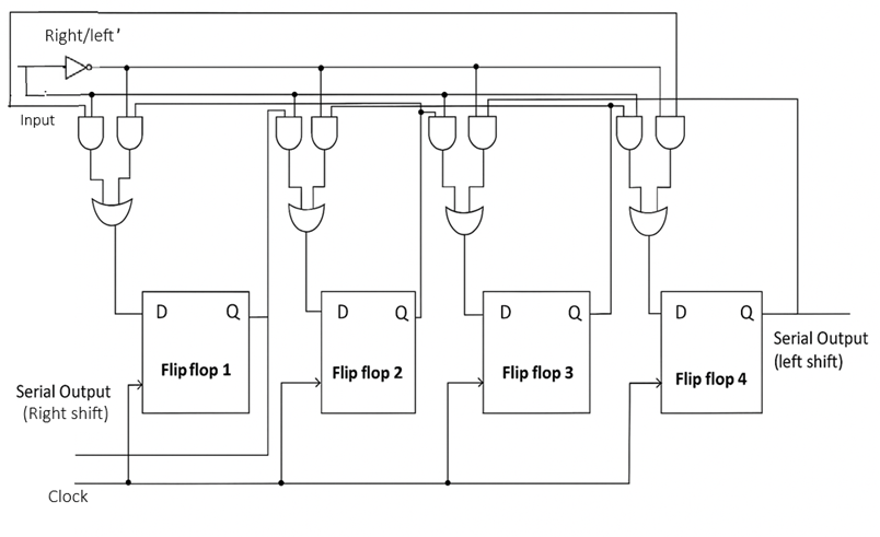
Figure 3: Bidirectional Shift Register circuit diagram showing multiplexer-based control for left/right shift operations. Reference: Advanced sequential processing implementation
A bidirectional shift register can shift data in either direction (left or right) based on a control signal. This versatility makes it useful in applications requiring flexible data movement and arithmetic operations.
Logic Operation
The register operates in three modes based on control signals:
- Right Shift (DIR = 0): Data shifts from left to right (MSB to LSB)
- Left Shift (DIR = 1): Data shifts from right to left (LSB to MSB)
- Parallel Load: Data can be loaded in parallel when enabled
Control Logic
For each flip-flop position, multiplexers select the appropriate data source:
For :
- Right Shift: Input =
- Left Shift: Input =
- Parallel Load: Input =
Logic Equations
For bit position :
Key Features
- Flexible data movement in both directions
- Multiplexer-based control for direction selection
- Can perform both logical and arithmetic shifts
- Essential for arithmetic operations
- Useful in data manipulation applications
Control Signal Operation
| LOAD | DIR | Operation |
|---|---|---|
| 1 | X | Parallel Load |
| 0 | 0 | Right Shift |
| 0 | 1 | Left Shift |
Applications
- Arithmetic operations (multiplication/division by 2)
- Barrel shifters in processors
- Data alignment in memory systems
- Digital signal processing
- Bit manipulation operations
Register Comparison and Selection
| Register Type | Control Inputs | Primary Function | Key Advantage |
|---|---|---|---|
| Basic Storage | CLK | Data storage | Simple, reliable |
| Parallel Load | CLK, LOAD | Conditional storage | Selective updating |
| Shift Register | CLK, Serial In | Serial data processing | Data conversion |
| Bidirectional | CLK, LOAD, DIR | Flexible shifting | Versatile operations |
Timing Analysis
Critical Timing Parameters
For all register types, proper timing must be maintained:
- Setup Time (): Data must be stable before clock edge
- Hold Time (): Data must remain stable after clock edge
- Clock-to-Output Delay (): Propagation delay through flip-flop
- Maximum Frequency ():
Clock Skew Considerations
In multi-bit registers, clock skew can cause timing violations:
- Positive Skew: Clock arrives later at some flip-flops
- Negative Skew: Clock arrives earlier at some flip-flops
- Mitigation: Balanced clock distribution networks
Practical Design Considerations
Power Consumption
- Dynamic Power:
- Static Power: Leakage current in modern CMOS processes
- Clock Power: Significant portion due to high fan-out
Noise Immunity
- Supply Voltage Variations: Affect timing and functionality
- Ground Bounce: Due to simultaneous switching
- Cross-talk: Between adjacent signal lines
Design Trade-offs
- Speed vs. Power: Faster registers consume more power
- Area vs. Functionality: More features require more silicon area
- Robustness vs. Performance: Conservative design vs. aggressive timing
Registers as Building Blocks
Registers serve as fundamental building blocks in digital systems and can be combined to create more complex circuits:
Counter Circuits
Registers can be configured with feedback logic to create counters:
- Binary Counters: Count in binary sequence using T or JK flip-flops
- Ring Counters: Circular shift of a single '1' bit through shift register
- Johnson Counters: Modified ring counters with inverted feedback
Memory Systems
Multiple registers can form basic memory structures:
- Register Files: Collections of registers for processor storage
- Cache Memory: Fast storage using register arrays with tag and data fields
- Buffer Memory: Temporary storage for data transfer between different clock domains
Data Path Components
Registers are essential in processor data paths:
- Pipeline Registers: Store intermediate results between processing stages
- Accumulator Registers: Store arithmetic operation results
- Address Registers: Hold memory addresses for data access
- Instruction Registers: Store the current instruction being executed
Advanced Register Applications
Processor Design
- Program Counter (PC): Special register storing next instruction address
- Stack Pointer (SP): Points to top of stack in memory
- Status Register: Stores processor flags (carry, zero, overflow, etc.)
- General Purpose Registers: For temporary data storage during computation
Communication Systems
- Transmit/Receive Buffers: Store data for serial communication
- Protocol State Machines: Use registers to track communication states
- Error Detection/Correction: Syndrome registers for ECC codes
Digital Signal Processing
- Delay Lines: Implement FIR filter structures using shift registers
- Circular Buffers: For continuous data streaming applications
- Coefficient Storage: For adaptive filter implementations
Key Design Considerations
Timing Requirements
- All registers must operate synchronously with the system clock
- Setup and hold times must be satisfied for reliable operation
- Clock distribution must minimize skew across large register arrays
Data Width Compatibility
- Register width must match the data path requirements
- Bus interface standards (8-bit, 16-bit, 32-bit, 64-bit)
- Endianness considerations for multi-byte data storage
Control Logic Design
- Appropriate control signals for loading and shifting operations
- Priority encoding for multiple control inputs
- Reset and initialization capabilities for system startup
Performance Optimization
- Efficient design to minimize power usage in large register arrays
- Speed optimization through careful flip-flop selection
- Area optimization using shared control logic where possible